Response of SiC photodiode was analytically simulated with diffusion transport equations for abrupt doping profiles, accounting for optical interference at the device surfaces.
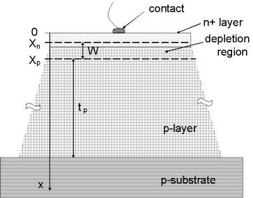 ◄ Structure of the UV photodiode (without passivation layers).
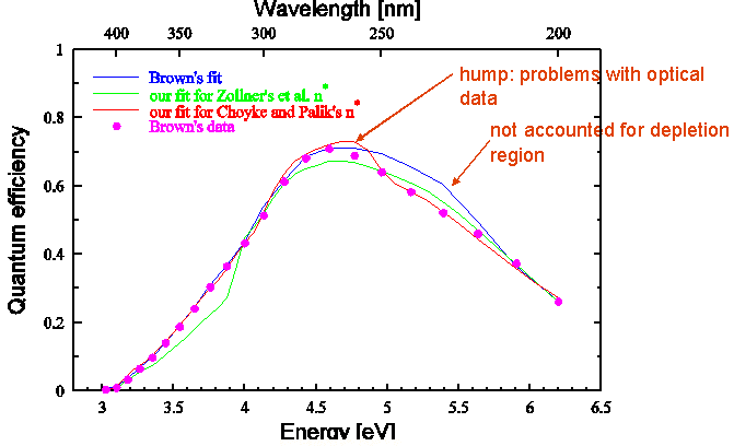 ◄ Fit of the quantum efficiency model to the
experimental data obtained by Brown et al. (1993, IEEE Tans. Electron. Devices 40, 325).
Device parameters: Nd=5E18 cm-3,
Na=3E17 cm-3, a top oxide thickness of
66 nm, a diffusion length of electrons of 1.76 microns, a surface
recombination velocity of 1.8E6 cm/s. Shown original fit of
Brown et al. did not account for charge space region at the p-n junction.
Our fit with optical data of Choyke and Palik
(1985, in Handbook of optical constants of solids, p.587.
Orlando: Academic, Ed. E. D. Palik) is better than one with optical data of
Zollner et al. (1999, J. Appl. Phys., 85, 8353).
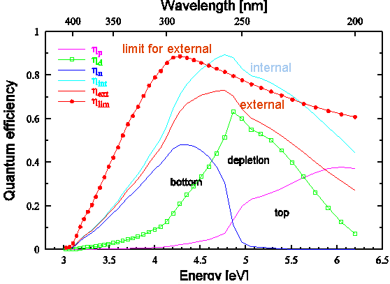 ◄ Components of quantum efficiency spectrum from
above fit: contributions of the bottom, depleted and top layers, total
internal efficiency (without losses from aperture, reflection at the
surfaces and transmission without absorption), external efficiency
and limit of external efficiency (for the case without losses due to charge
carrier recombination).
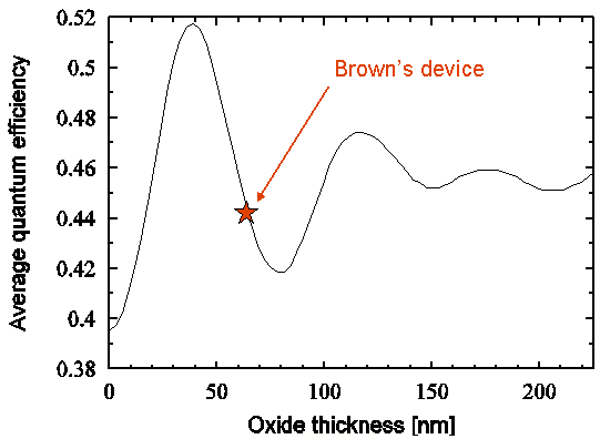 ◄ Effect of SiO2 top passivation layer on the
quantum efficiency, which is shown as energy averaged in the wavelength range
200-400 nm.
Parameters of the device are those above except the oxide
thickness. Optical modeling is based on the Lambert-Beer's absorption formula
and thin film stack treatment with usage the Fresnel's coefficients.
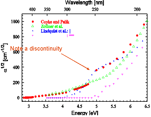 ◄ Anisotropy of optical properties of 6H-SiC as it
appears in absorption coefficient.
Data of Choyke and Palik are
compiled from different sources. Absorption derived from Lindquist's
et al. data (2001, Appl. Phys. Lett. 78, 2715) is shown for
components of 6H-SiC dielectric function parallel (blue symbols)
and perpendicular (pink symbols) to the hexagonal lattice axis.
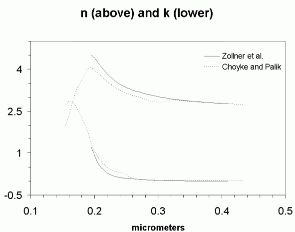 ◄ Complex refractive coefficient from Choyke and Palik
(text file here), and Zollner et al. data.